LEE-BED - the "one-stop shop" for the printed electronics of tomorrow

Logo LEE-BED
© LEE-BED H2020 project
LEE-BED brings together leading research and industry partners across Europe in a unique open innovation test bed.

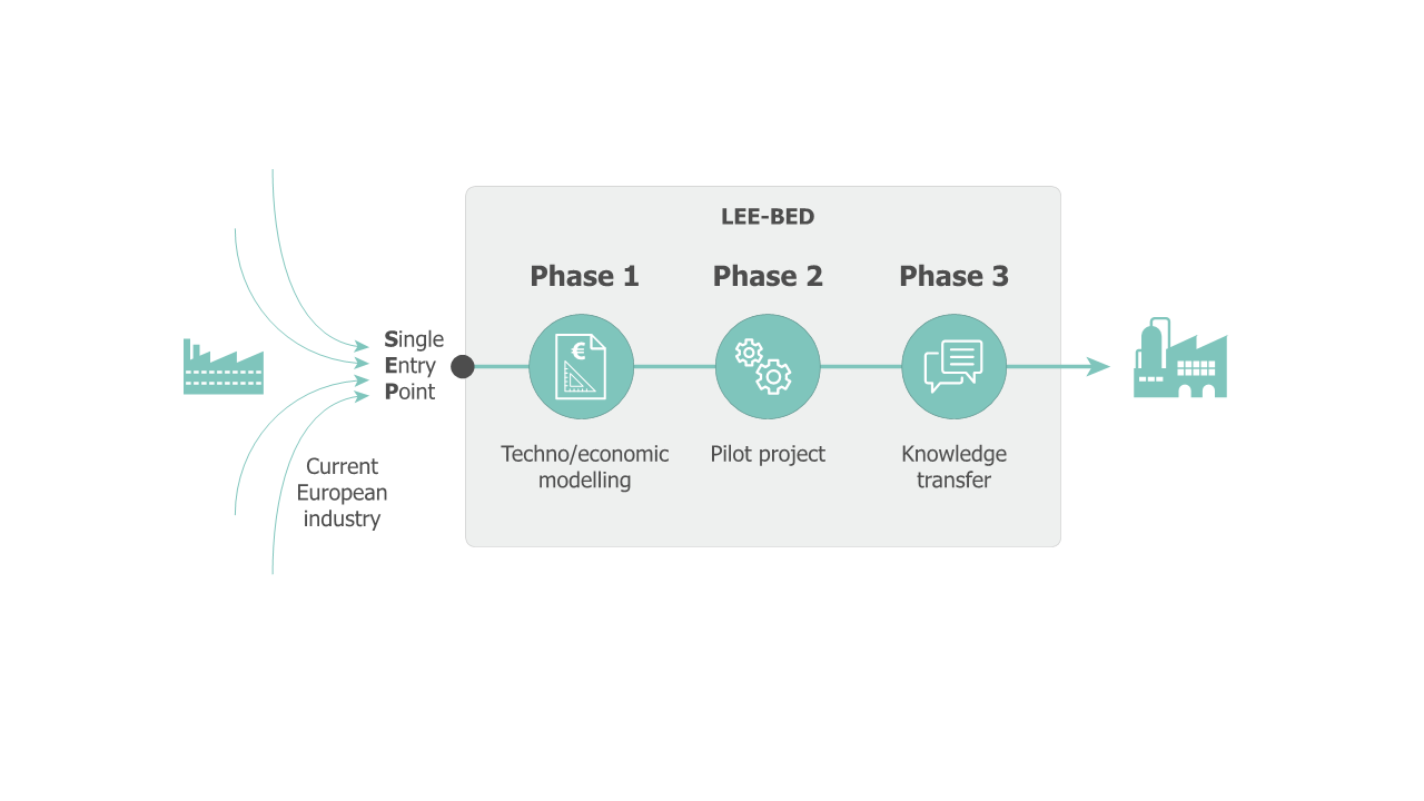
LEE-BED is an EU-funded Open Innovation Test Bed which provides European companies with easy, risk-free access to printed and embedded electronics. Via the user-friendly single entry point (SEP), customers with and without experience in the technology are granted direct access to leading European R&D facilities in the field of printed electronics. The process is simple. To start with, the technological and economic aspects of ideas are evaluated in three phases. Then, prototypes are built on selected test beds and, finally, know-how is transferred from the project partners to customers. The LEE-BED one-stop shop is thus the perfect incubator for advancing the development and spread of nano-based printed electronics.
Project goals

The aim of the project is to provide European companies with easy access to printed electronics. After registering at the web-based SEP, customers receive a comprehensive techno-economic analysis. Quickly and reliably, this identifies and evaluates advantages and obstacles on the path to implementation:

  • Technology
  • Economics
  • Health and Safety
  • Environmental sustainability
  • Patent situation
  • Funding mechanisms

In Phase 2, if the results of the evaluation are positive, prototypes up to TRL7 can be developed in pilot projects. Test beds for nanomaterials, formulations and components are available for this. In this way, the most feasible technical implementations can be tested in practice without high investment costs or development expertise on the part of the customer.

Lastly, in Phase 3, a final knowledge transfer takes place that provides a complete implementation roadmap and supports sustainable business models.

Current project status

So far in the project, the techno-economic services for LEE-BED Phase 1 have been developed under the leadership of scientists at Fraunhofer IBP and validated with the help of internal partners from industry. The use cases positively evaluated in the study are currently being pursued in Phase 2, in which prototypes are being built on test beds and functional tests carried out.

To quantify the aspects of environmental sustainability that were investigated in Phase 1 even more precisely, the team of Fraunhofer IBP experts is also presently studying the environmental impact of the various manufacturing processes and test beds.

Currently, interested parties from industry have the opportunity to test all three LEE-BED phases. For this, free Phase 1 evaluations will be carried out for ten test customers by 30.09.2021 (further information: www.lee-bed.eu/sign-up).

The aim is to establish a commercially viable concept for the LEE-BED open innovation test bed by the end of the project in December 2022.

Project partners

  • Danish Technological Institute (coordination)
  • Centre for Process Innovation
  • Nederlandse Organisatie Voor Toegepast Natuurwetenschappelijk Onderzoek 
  • Eindhoven University of Technology
  • RISE AB
  • Instituto Tecnológico del Embalaje, Transporte y Logística
  • Fraunhofer Institute for Building Physics IBP  
  • Fraunhofer Institute for Integrated Circuits IIS  
  • Commissariat à l'énergie atomique et aux énergies Alternatives (CEA)
  • VSParticle B.V.
  • Sustainable Innovations Europe SL
  • AXIA Innovation UG
  • Teknologi & Produkt Udvikling AS
  • MAIER SCOOP
  • Grafietic SL
  • ACCIONA construcción SA
  • Global Equity & Corporate Consulting SL
  • D. SWAROVSKI KG
Three-phase process LEE-BED
© LEE-BED H2020 project
After registering at the single entry point, customers go through a three-phase process to realize their ideas.
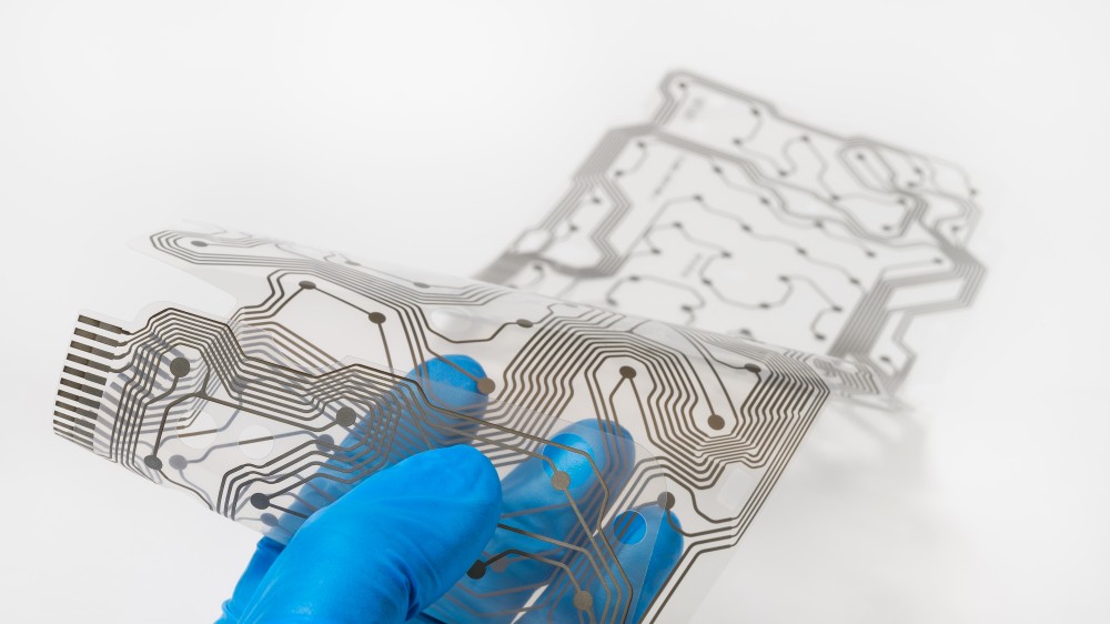
Printed electronic circuits
© Shutterstock / KPixMining
Printed electronic circuits based on a conductive ink with silver nanoparticles.